Support for the Sipeed Longan Nano board. More...
Detailed Description
Support for the Sipeed Longan Nano board.
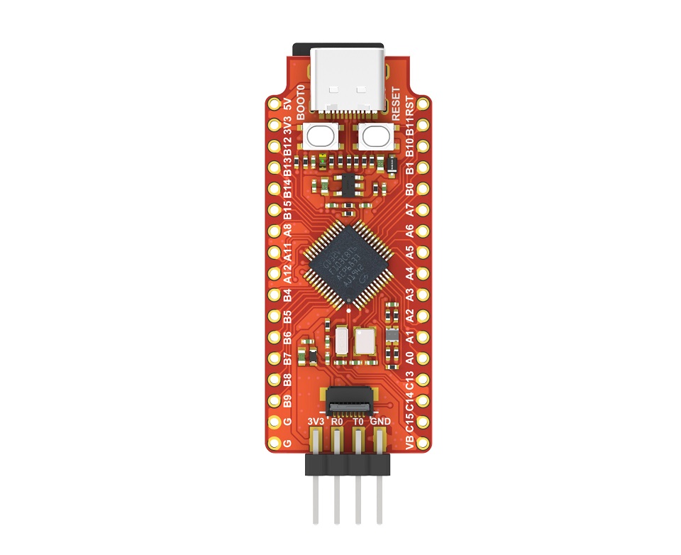
Sipeed Longan Nano
Overview
The Sipeed Longan Nano is a development board for the GigaDevice GD32VF103CBT6 MCU with the following on-board components:
- GD32VF103CBT6 RISC-V MCU @108MHz
- USB Type C
- TF card slot
- 3 user LEDs
- 0.96" TFT display 160 x 80 pixel (optional)
Hardware
| MCU | GD32VF103CBT6 | Supported |
|---|---|---|
| Family | RISC-V with ECLIC | |
| Vendor | GigaDevice | |
| RAM | 32 kByte | |
| Flash | 128 KByte | |
| Frequency | 108 MHz | |
| Power Modes | 3 (Sleep, Deep Sleep, Standby) | yes |
| GPIOs | 37 | yes |
| Timers | 5 x 16-bit timer | yes |
| RTC | 1 x 32-bit counter, 20-bit prescaler | yes |
| WDT | 2 x 12-bit counter, 3-bit prescaler | yes |
| ADC | 2 x 12-bit units, 16 channels @ 1 Msps | yes |
| DAC | 2 x 12-bit channel | yes |
| UART | - | yes |
| USART | 3 | yes |
| SPI | 3 | yes |
| I2C | 2 x Fast Mode 400 kHz | yes |
| I2S | 2 | no |
| CAN | 2 x CAN 2.0B with up to 1 Mbps | no |
| PWM | 6 Channels | yes |
| USB | 1 x USB FS OTG | yes |
| Vcc | 3.0V - 3.6V | |
| Datasheet | Datasheet | |
| Reference Manual | Reference Manual | |
| Board Manual | Board Manual | |
| Board Schematic | Board Schematic |
Pin Layout / Configuration
The general pin layout is shown below.
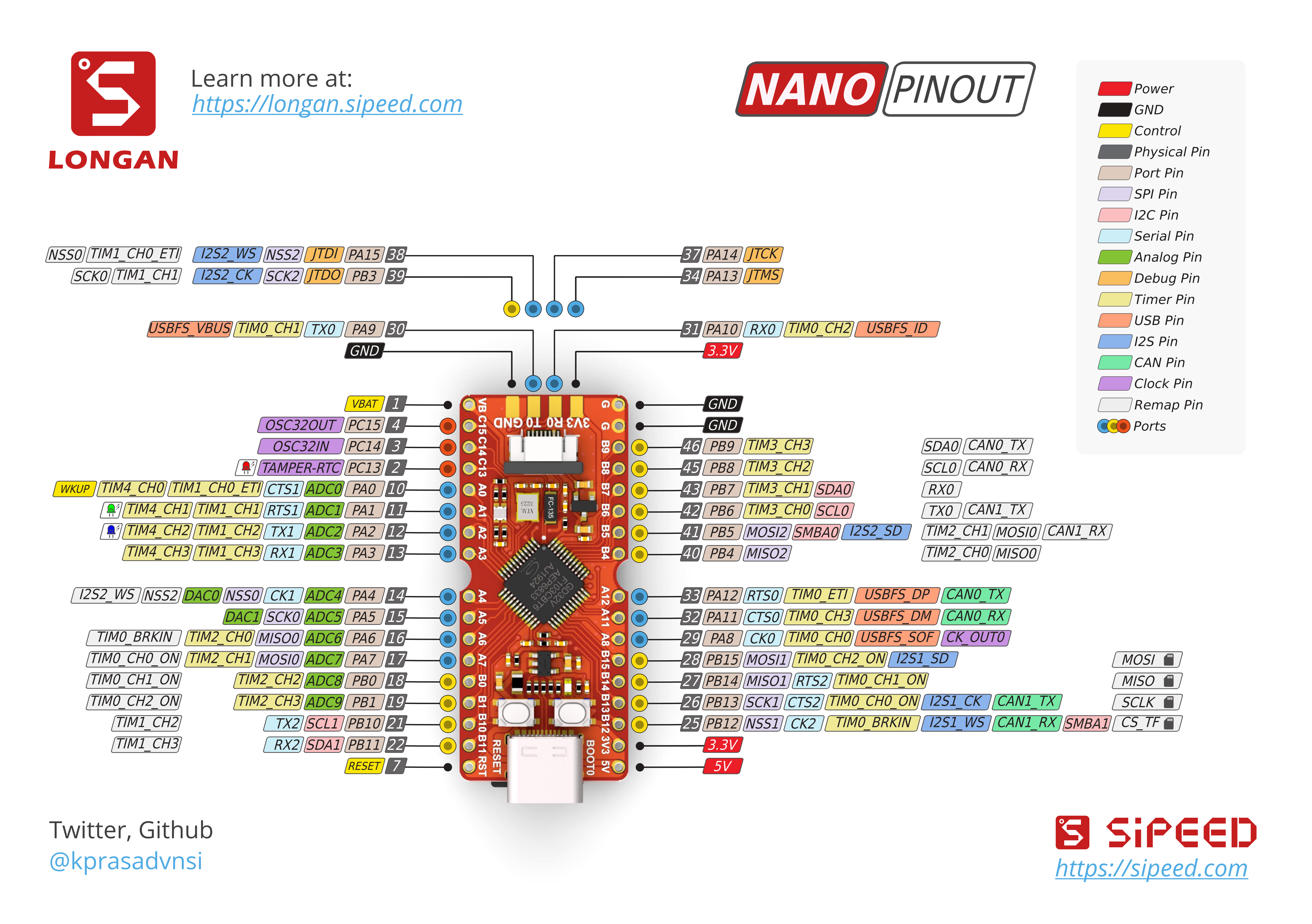
The following tables show the connection of the on-board components with the MCU pins and their configuration in RIOT sorted by RIOT peripherals and by pins.
| RIOT Peripheral | MCU Pin | MCU Peripheral | Board Function | Remark |
|---|---|---|---|---|
| ADC_LINE(0) | PA0 | ADC01_IN0 | ||
| ADC_LINE(1) | PA3 | ADC01_IN3 | ||
| ADC_LINE(2) | - | ADC01_IN16 | internal Temperature channel | |
| ADC_LINE(3) | - | ADC01_IN17 | internal VFEF channel | |
| ADC_LINE(4)* | PA4 | ADC01_IN4 | N/A if DAC is used | |
| ADC_LINE(5)* | PB0 | ADC01_IN8 | TFT RS | N/A if TFT is used |
| ADC_LINE(6)* | PB1 | ADC01_IN9 | TFT RST | N/A if TFT is used |
| ADC_LINE(7)* | PA6 | ADC01_IN6 | N/A if TFT/SPI_DEV(1) is used | |
| ADC_LINE(8)* | PA7 | ADC01_IN7 | N/A if TFT/SPI_DEV(1) is used | |
| ADC_LINE(9)* | PA5 | ADC01_IN5 | N/A if TFT/SPI_DEV(1)/DAC used | |
| BTN0 | PA8 | BOOT0 | BOOT | |
| DAC_LINE(0) | PA4 | DAC0 | ||
| DAC_LINE(1)* | PA5 | DAC1 | N/A if TFT is used | |
| GPIO_PIN(1, 2) | PB2 | TFT CS | ||
| I2C_DEV(0) SCL | PB6 | I2C0 SCL | ||
| I2C_DEV(0) SDA | PB7 | I2C0 SDA | ||
| I2C_DEV(1) SCL | PB10 | I2C1 SCL | ||
| I2C_DEV(1) SDA | PB11 | I2C1 SDA | ||
| LED0 | PC13 | LED red | ||
| LED1 | PA1 | LED green | ||
| LED2 | PA2 | LED blue | ||
| PWM_DEV(0) CH0 | PA1 | LED green | ||
| PWM_DEV(0) CH1 | PA2 | LED blue | ||
| PWM_DEV(1) CH0* | PB8 | N/A if CAN is used | ||
| PWM_DEV(1) CH1* | PB9 | N/A if CAN is used | ||
| SPI_DEV(0) CS | PB12 | SPI1 CS | SD CS | |
| SPI_DEV(0) SCLK | PB13 | SPI1 SCLK | SD SCK | |
| SPI_DEV(0) MISO | PB14 | SPI1 MISO | SD MISO | |
| SPI_DEV(0) MOSI | PB15 | SPI1 MOSI | SD MOSI | |
| SPI_DEV(1) CS | PB5 | SPI0 CS | ||
| SPI_DEV(1) SCLK | PA5 | SPI0 SCLK | TFT SCL | |
| SPI_DEV(1) MISO | PA6 | SPI0 MISO | ||
| SPI_DEV(1) MOSI | PA7 | SPI0 MOSI | TFT SDA | |
| UART_DEV(0) TX | PA9 | USART0 TX | UART TX | |
| UART_DEV(0) RX | PA10 | USART0 RX | UART RX |
(*) The availability of these peripherals depend on the use of other peripherals.
- Note
- For the Sipeed Longan Nano board version with TFT display, the
sipeed-longan-nano-tftboard definition has to be used.BOARD=sipeed-longan-nano-tft make ...
| Pin | Board Function | RIOT Function 1 | RIOT Function 2 | RIOT Function 3 |
|---|---|---|---|---|
| PA0 | ADC_LINE(0) | |||
| PA1 | LED green | PWM_DEV(0) CH0 | LED0 | |
| PA2 | LED blue | PWM_DEV(0) CH1 | LED1 | |
| PA3 | ADC_LINE(1) | |||
| PA4 | ADC_LINE(4)* | DAC_LINE(0) | ||
| PA5 | TFT SCL | SPI_DEV(1) SCLK | ADC_LINE(9)* | DAC_LINE(1)* |
| PA6 | SPI_DEV(1) MISO | ADC_LINE(7)* | ||
| PA7 | TFT SDA | SPI_DEV(1) MOSI | ADC_LINE(8)* | |
| PA8 | BOOT | BTN0 | ||
| PA9 | UART_DEV(0) TX | |||
| PA10 | UART_DEV(0) RX | |||
| PA11 | USB D- | |||
| PA12 | USB D+ | |||
| PA13 | JTAG TMS | |||
| PA14 | JTAG TCK | |||
| PA15 | JTAG TDI | |||
| PB0 | TFT RS | ADC_LINE(5)* | ||
| PB1 | TFT RST | ADC_LINE(6)* | ||
| PB2 | TFT CS | |||
| PB3 | JTAG TDO | |||
| PB4 | JTAG NRST | |||
| PB5 | SPI_DEV(1) CS | |||
| PB6 | I2C_DEV(0) SCL | |||
| PB7 | I2C_DEV(0) SDA | |||
| PB8 | PWM_DEV(1) CH0 | |||
| PB9 | PWM_DEV(1) CH1 | |||
| PB10 | I2C_DEV(1) SCL | |||
| PB11 | I2C_DEV(1) SDA | |||
| PB12 | SD CS | SPI_DEV(0) CS | ||
| PB13 | SD SCK | SPI_DEV(0) SCLK | ||
| PB14 | SD MISO | SPI_DEV(0) MISO | ||
| PB15 | SD MOSI | SPI_DEV(0) MOSI | ||
| PC13 | LED red | LED2 | ||
| PC14 | OSC32IN | |||
| PC15 | OSC32OUT | |||
| - | Temperature | ADC_LINE(2) | ||
| - | VREF | ADC_LINE(3) |
(*) The availability of these peripherals depend on the use of other peripherals.
- Note
- Since the availability of
ADC_LINE(4)toADC_LINE(9)depends on other peripheral configurations, their index may vary.
Flashing the Device
Using the DFU bootloader
The board is flashed via the in-ROM DFU bootloader by default. To enter bootloader mode, hold the BOOT0 button while pressing the RESET button.
After flashing you need to leave bootloader mode again by pressing the RESET button.
- Note
- For the Sipeed Longan Nano board version with TFT display, the
sipeed-longan-nano-tftboard definition has to be used.BOARD=sipeed-longan-nano-tft make -C examples/basic/hello-world flash
Using an external debug adapter
The board can also be flashed via a JTAG interface with OpenOCD (at least release version 0.12.0). By default, an FTDI adapter according to the configuration defined in interface/openocd-usb.cfg is assumed.
To use an FTDI adapter with a different configuration, the configuration can be defined using the variable OPENOCD_FTDI_ADAPTER, for example:
If another adapter is used, it can be specified using variable OPENOCD_DEBUG_ADAPTER, for example for a Segger J-Link adapter:
Using the TFT Display
To use the display of the Sipeed Longan Nano board version with TFT display, the sipeed_longan_nano_tft board definition has to be used, for example:
Accessing STDIO
By default, the stdio is provided by the USBUS CDC ACM module stdio_cdc_acm. This interface is mapped to /dev/ttyACM<n> on a Linux host, where <n> is the index of the CDC ACM interface, which is 0 by default.
To use the first UART interface for stdio instead, the stdio_uart module has to be enabled:
The stdio is then directly accessible through the first UART interface. If an external USB-to-UART interface is used, this interface is mapped to /dev/ttyUSB<n> on a Linux host, where <n> is the index of the UART interface, which is 0 by default.
Use the term target to connect to the board using /dev/ttyUSB0:
If the UART interface index of the USB-to-UART interface is not 0, use the following command to connect:
Files | |
| file | board.h |
| Board specific definitions for the Sipeed Longan Nano board. | |
| file | gpio_params.h |
| Configuration of SAUL mapped GPIO pins. | |
| file | periph_conf.h |
| Board specific definitions for the Sipeed Longan Nano board. | |
