MSB-A2
Support for the ScatterWeb MSB-A2 board
Support for the ScatterWeb MSB-A2 board
Overview
Hardware
| MCU: | LPC2387 ARM7-TDMI |
|---|---|
| RAM: | 96KiB |
| Flash: | 512KiB |
More info
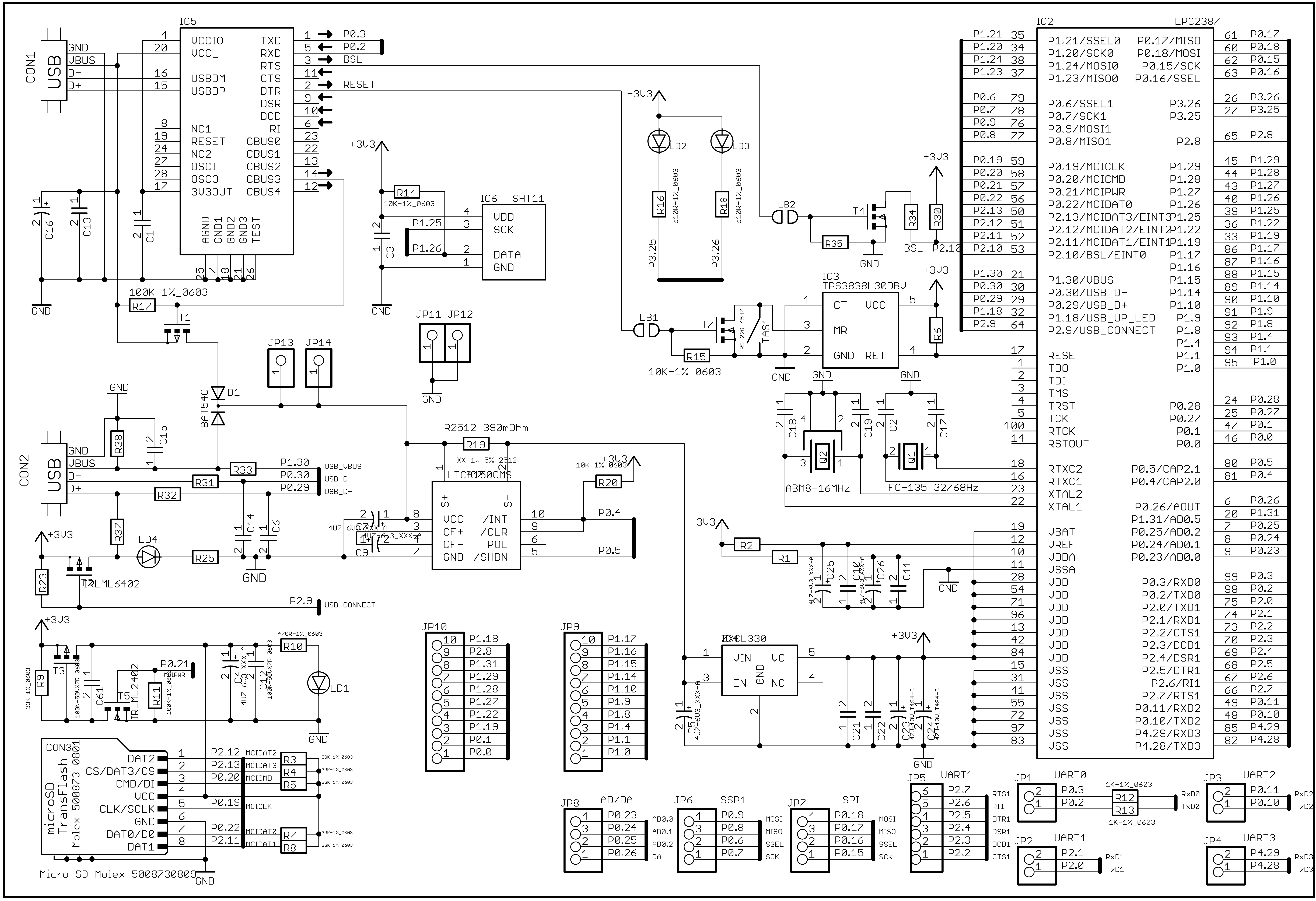
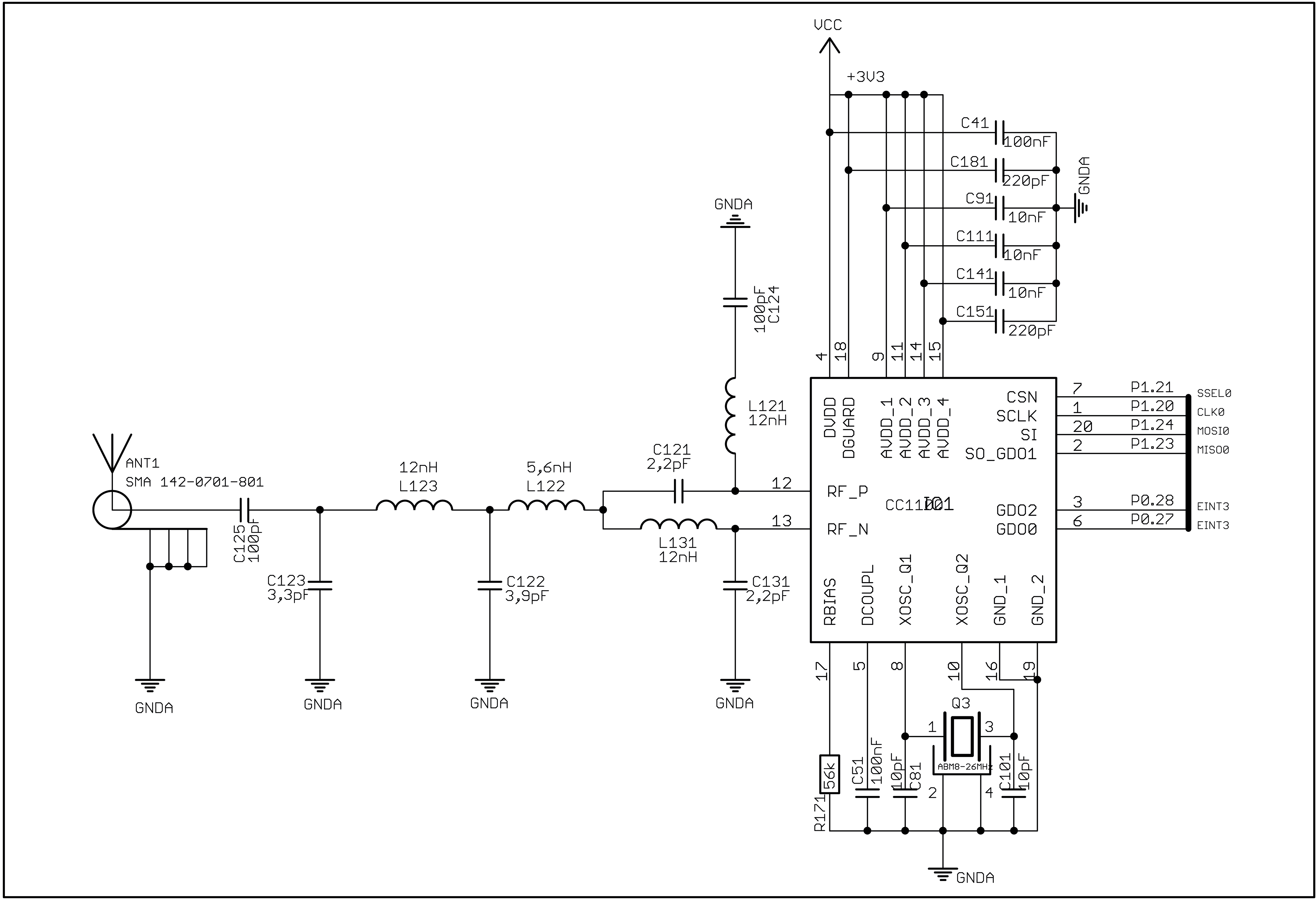
Board Schematics
Circuit Diagrams
MSB-A2 page @ Freie Universität Berlin/CST
Flashing
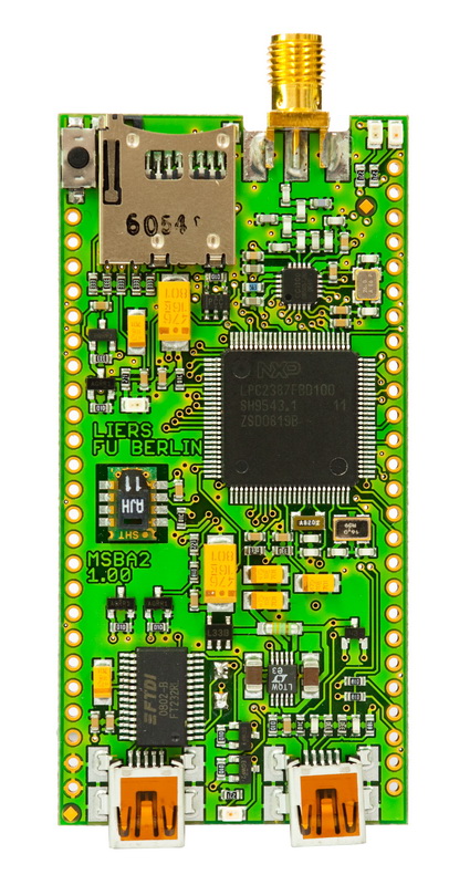
The MSB-A2 is programmed via an ISP bootloader over UART. The board includes an FTDI USB-TTL converter, which is connected to the left USB Mini-B connector (see picture above). Connect the MSB-A2 using that connector to your PC and run from within the folder of your application to flash:
BOARD=msba2 make flashYou’ll notice that during the first invocation takes a bit longer, as the tool
lpc2k_pgm used to flash the MSB-A2 is also compiled.
You can connect to the shell by running:
BOARD=msba2 make termDebugging
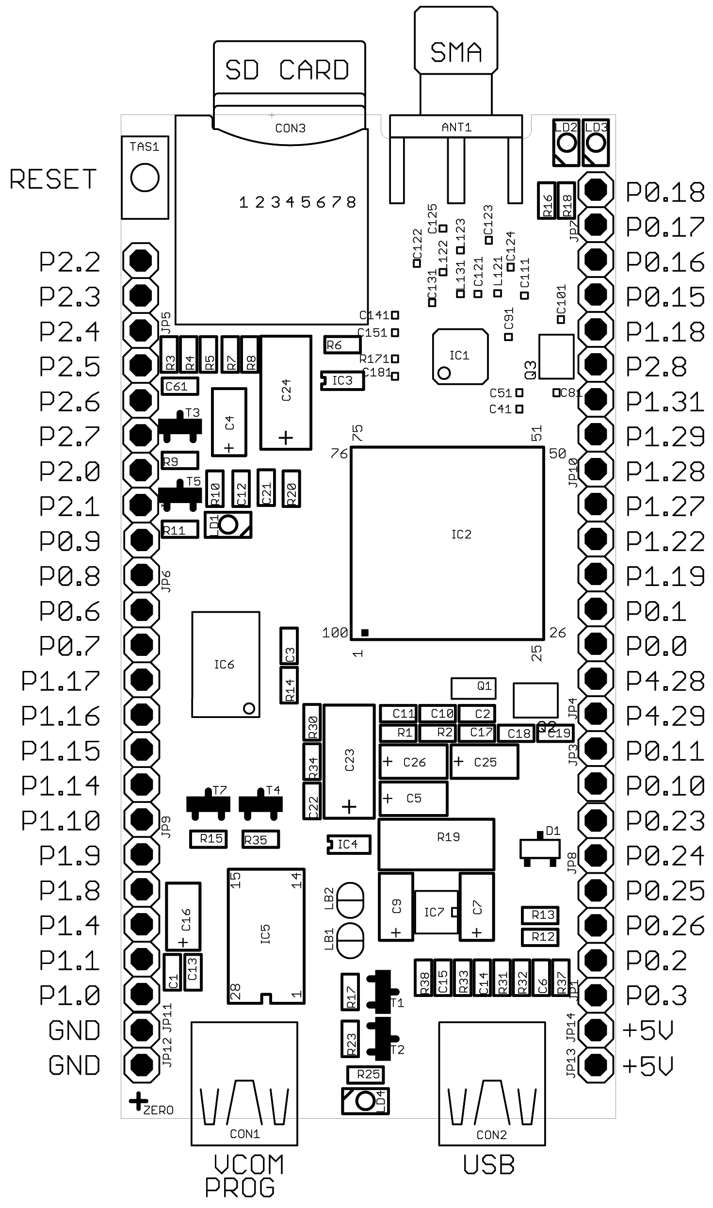
Some rigorous hardware modification is needed to access the JTAG interface of the MSB-A2.
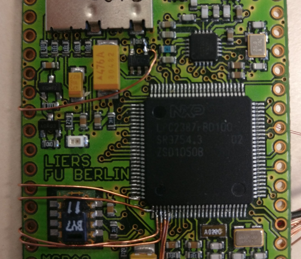
The following wires need to be soldered on:
| Signal | Place |
|---|---|
| JTAG-TDO | IC2, Pin 1 |
| JTAG-TDI | IC2, Pin 2 |
| JTAG-TMS | IC2, Pin 3 |
| JTAG-TRST | IC2, Pin 4 |
| JTAG-TCK | IC2, Pin 5 |
| JTAG-RTCK (*) | IC2, Pin 100 |
| RESET | right pad of R6 (easier to solder) or IC2, Pin 17 |
| GND | The bottom left through-hole pad |
(*) You can safely omit the connection to JTAG-RTCK.
As debugger an FT2232HL is used, the cheapest version costs less 10€ (often nicknamed CJMCU-2232HL).
Connect as follows:
| FT2232HL | MSB-A2 |
|---|---|
| GND | GND |
| AD0 | JTAG-TCK |
| AD1 | JTAG-TDI |
| AD2 | JTAG-TDO |
| AD3 | JTAG-TMS |
| AD4 | JTAG-TRST |
| AD5 | RESET |
Once this is done, debugging is as simple as running:
BOARD=msba2 make debugFlashing via OpenOCD
Theoretically you should be able to flash also via JTAG. But do not expect this to be faster. Also: Do you really want to risk bricking the MSB-A2 you spend so much time to modify? The author of this text surely didn’t want to risk that…