ESP-WROVER-KIT V3
Support for for Espressif ESP-WROVER-KIT V3
Support for for Espressif ESP-WROVER-KIT V3 @author Gunar Schorcht gunar@schorcht.net
\section esp32_wrover_kit ESP-WROVER-KIT V3
Overview
The Espressif ESP-WROVER-KIT is a development board that uses the ESP32-WROVER module which includes a built-in 4 MByte SPI RAM. Most important features of the board are
- Micro-SD card interface
- OV7670 camera interface
- 3.2” SPI LCD panel
- RGB LED
- USB bridge with JTAG interface
- external 32.768 kHz crystal for RTC
Furthermore, many GPIOs are broken out for extension. The USB bridge based on FDI FT2232HL provides a JTAG interface for OCD debugging through the USB interface.
Hardware
MCU
Most features of the board are provided by the ESP32 SoC. For detailed information about the ESP32, see section esp32_mcu_esp32 “MCU ESP32”.
Board Configuration
ESP-WROVER-KIT has the following on-board components
- Micro-SD card interface
- OV7670 camera interface
- 3.2” SPI LCD panel
- RGB LED
- USB bridge with JTAG interface
- external 32.768 kHz crystal for RTC
The following table shows the default board configuration sorted according to the defined functionality of GPIOs for different hardware options. This configuration can be overridden by esp32_application_specific_configurations .
These abbreviations are used in subsequent tables:
SDC = SD-Card interface is used (module periph_sdmmc is enabled)
CAM = Camera is plugged in/used
| Function | None | SDC | CAM | SDC + CAM | Remarks | Configuration |
|---|---|---|---|---|---|---|
ADC_LINE(0) | GPIO34 | GPIO34 | - | - | CAMERA_D6 | esp32_adc_channels |
ADC_LINE(1) | GPIO35 | GPIO35 | - | - | CAMERA_D7 | esp32_adc_channels |
ADC_LINE(2) | GPIO36 | GPIO36 | - | - | CAMERA_D4 | esp32_adc_channels |
ADC_LINE(3) | GPIO39 | GPIO39 | - | - | CAMERA_D5 | esp32_adc_channels |
PWM_DEV(0):0 / LED0 | GPIO0 | GPIO0 | - | - | LED_RED / CAMERA_RESET | esp32_pwm_channels |
PWM_DEV(0):1 / LED2 | GPIO4 | GPIO4 | - | - | LED_BLUE / CAMERA_D0 | esp32_pwm_channels |
LED1 | GPIO2 | GPIO2 | GPIO2 | GPIO2 | LED_GREEN | |
I2C_DEV(0):SCL | GPIO27 | GPIO27 | GPIO27 | GPIO27 | CAMERA_SIO_C | esp32_i2c_interfaces |
I2C_DEV(0):SDA | GPIO26 | GPIO26 | GPIO26 | GPIO26 | CAMERA_SIO_D | esp32_i2c_interfaces |
UART_DEV(0):TX | GPIO1 | GPIO1 | GPIO1 | GPIO1 | esp32_uart_interfaces | |
UART_DEV(0):RX | GPIO3 | GPIO3 | GPIO3 | GPIO3 | esp32_uart_interfaces | |
SDMMC_DEV(0):CLK | GPIO14 | GPIO14 | - | - | SD-Card | esp32_sdmmc_interfaces |
SDMMC_DEV(0):CMD | GPIO15 | GPIO | - | - | SD-Card | esp32_sdmmc_interfaces |
SDMMC_DEV(0):DAT0 | GPIO2 | GPIO2 | - | - | SD-Card | esp32_sdmmc_interfaces |
SDMMC_DEV(0):DAT1 | GPIO4 | GPIO4 | - | - | SD-Card | esp32_sdmmc_interfaces |
SDMMC_DEV(0):DAT2 | GPIO12 | GPIO | - | - | SD-Card | esp32_sdmmc_interfaces |
SDMMC_DEV(0):DAT3 | GPIO13 | GPIO | - | - | SD-Card | esp32_sdmmc_interfaces |
SPI_DEV(0):SCK | GPIO14 | GPIO14 | GPIO14 | GPIO14 | HSPI: SD-Card / Peripherals | esp32_spi_interfaces |
SPI_DEV(0):MOSI | GPIO15 | GPIO15 | GPIO15 | GPIO15 | HSPI: SD-Card / Peripherals | esp32_spi_interfaces |
SPI_DEV(0):CS0 | GPIO13 | GPIO13 | GPIO13 | GPIO13 | HSPI: SD-Card CS | esp32_spi_interfaces |
SPI_DEV(1)/LCD:SCK | GPIO19 | GPIO19 | - | - | VSPI: LCD / CAMERA_D3 | esp32_spi_interfaces |
SPI_DEV(1)/LCD:MOSI | GPIO23 | GPIO23 | - | - | VSPI: LCD / CAMERA_HREF | esp32_spi_interfaces |
SPI_DEV(1)/LCD:MISO | GPIO25 | GPIO25 | - | - | VSPI: LCD / CAMERA_VSYNC | esp32_spi_interfaces |
SPI_DEV(1)/LCD:CS0 | GPIO22 | GPIO22 | - | - | VSPI: LCD / CAMERA_PCLK | esp32_spi_interfaces |
LCD_LED | GPIO5 | GPIO5 | - | - | CAMERA_D1 | |
LCD_SCL | GPIO19 | GPIO19 | - | - | CAMERA_D3 | |
LCD_MOSI | GPIO23 | GPIO23 | - | - | CAMERA_HREF | |
LCD_MISO | GPIO25 | GPIO25 | - | - | CAMERA_VSYNC | |
LCD_CS | GPIO22 | GPIO22 | - | - | CAMERA_PCLK | |
LCD_D/C | GPIO21 | GPIO21 | - | - | CAMERA_XCLK | |
LCD_RESET | GPIO18 | GPIO18 | - | - | CAMERA_D2 | |
CAMERA_D0 | - | - | GPIO4 | GPIO4 | ||
CAMERA_D1 | - | - | GPIO5 | GPIO5 | ||
CAMERA_D2 | - | - | GPIO18 | GPIO18 | ||
CAMERA_D3 | - | - | GPIO19 | GPIO19 | ||
CAMERA_D4 | - | - | GPIO36 | GPIO36 | ||
CAMERA_D5 | - | - | GPIO39 | GPIO39 | ||
CAMERA_D6 | - | - | GPIO34 | GPIO34 | ||
CAMERA_D7 | - | - | GPIO35 | GPIO35 | ||
CAMERA_XCLK | - | - | GPIO21 | GPIO21 | ||
CAMERA_PCLK | - | - | GPIO22 | GPIO22 | ||
CAMERA_HREF | - | - | GPIO23 | GPIO23 | ||
CAMERA_VSYNC | - | - | GPIO25 | GPIO25 | ||
CAMERA_SIO_D | - | - | GPIO26 | GPIO26 | ||
CAMERA_SIO_C | - | - | GPIO27 | GPIO27 | ||
CAMERA_RESET | - | - | GPIO0 | GPIO0 |
Following table shows the default board configuration sorted by GPIOs depending on used hardware.
| Pin | None | SDC 4-bit | CAM | SDC 1-bit + CAM | Remarks |
|---|---|---|---|---|---|
| GPIO0 | PWM_DEV(0):0 / LED0 | PWM_DEV(0):0 / LED0 | CAMERA_RESET | CAMERA_RESET | |
| GPIO1 | UART_DEV(0):TX | UART_DEV(0):TX | UART_DEV(0):TX | UART_DEV(0):TX | |
| GPIO2 | SPI_DEV(0):MISO / LED1 | SDMMC_DEV(0):DAT0 | SPI_DEV(0):MISO | SDMMC_DEV(0):DAT0 | HSPI |
| GPIO3 | UART_DEV(0):RX | UART_DEV(0):RX | UART_DEV(0):RX | UART_DEV(0):RX | |
| GPIO4 | PWM_DEV(0):1 / LED2 | SDMMC_DEV(0):DAT1 | CAMERA_D0 | CAMERA_D0 | |
| GPIO5 | LCD LED | LCD_LED | CAMERA_D1 | CAMERA_D1 | |
| GPIO6 | Flash CLK | Flash CLK | Flash CLK | Flash CLK | |
| GPIO7 | Flash SD0 | Flash SD0 | Flash SD0 | Flash SD0 | |
| GPIO8 | Flash SD1 | Flash SD1 | Flash SD1 | Flash SD1 | |
| GPIO9 | |||||
| GPIO10 | |||||
| GPIO11 | Flash CMD | Flash CMD | Flash CMD | Flash CMD | |
| GPIO12 | SDMMC_DEV(0):DAT2 | ||||
| GPIO13 | SPI_DEV(0):CS0 | SDMMC_DEV(0):DAT3 | SPI_DEV(0):CS0 | HSPI / SPI SD-Card CS | |
| GPIO14 | SPI_DEV(0):SCK | SDMMC_DEV(0):CLK | SPI_DEV(0):SCK | HSPI | |
| GPIO15 | SPI_DEV(0):MOSI | SDMMC_DEV(0):CMD | SPI_DEV(0):MOSI | HSPI | |
| GPIO16 | N/A | N/A | N/A | N/A | see below |
| GPIO17 | N/A | N/A | N/A | N/A | see below |
| GPIO18 | LCD_RESET | LCD_RESET | LCD_RESET | CAMERA_D2 | |
| GPIO19 | SPI_DEV(1)/LCD:SCK | SPI_DEV(1)/LCD:SCK | SPI_DEV(1)/LCD:SCK | CAMERA_D3 | VSPI |
| GPIO21 | LCD_D/C | LCD_D/C | LCD_D/C | CAMERA_XCLK | |
| GPIO22 | SPI_DEV(1)/LCD:CS | SPI_DEV(1)/LCD:CS0 | SPI_DEV(1)/LCD:CS0 | CAMERA_PCLK | VSPI |
| GPIO23 | SPI_DEV(1)/LCD:MOSI | SPI_DEV(1)/LCD:MOSI | SPI_DEV(1)/LCD:MOSI | CAMERA_HREF | VSPI |
| GPIO25 | SPI_DEV(1)/LCD:MISO | SPI_DEV(1)/LCD:MISO | SPI_DEV(1)/LCD:MISO | CAMERA_VSYNC | VSPI |
| GPIO26 | I2C_DEV(0):SDA | I2C_DEV(0):SDA | I2C_DEV(0):SDA | I2C_DEV(0)/CAMERASIO_D:SDA | |
| GPIO27 | I2C_DEV(0):SCL | I2C_DEV(0):SCL | I2C_DEV(0):SCL | I2C_DEV(0)/CAMERASIO_C:SCL | |
| GPIO32 | N/A | N/A | N/A | N/A | see below |
| GPIO33 | N/A | N/A | N/A | N/A | see below |
| GPIO34 | ADC_LINE(0) | ADC_LINE(0) | ADC_LINE(0) | CAMERA_D6 | |
| GPIO35 | ADC_LINE(1) | ADC_LINE(1) | ADC_LINE(1) | CAMERA_D7 | |
| GPIO36 | ADC_LINE(2) | ADC_LINE(2) | ADC_LINE(2) | CAMERA_D4 | |
| GPIO39 | ADC_LINE(3) | ADC_LINE(3) | ADC_LINE(3) | CAMERA_D5 |
@note
- SPI_DEV(0) uses the HSPI interface with the GPIO2 pin as the MISO signal. Since GPIO2 has bootstrapping functionality, it might be necessary to to press the Boot button for flashing RIOT when the SD card or the peripheral hardware is attached to this SPI interface.
- GPIO0 cannot be used as SPI CS signal for external hardware connected to SPI_DEV(0). The reason for this is that the LEDs on this board are high-active and the default state of the LEDs after power-up causes a low level on the corresponding GPIO outputs.
- GPIO2 cannot be used as PWM_DEV(0) channel 1 / LED0 when SPI_DEV(0) is used in any way. Reason is that GPIO2 is the MISO signal when SPI_DEV(0) is used and is therefore an input. PWM channels are outputs.
- It might be necessary to remove the SD card or the peripheral hardware attached to the SPI_DEV(0) interface for flashing RIOT. Reason is that the SPI_DEV(0) interface uses the HSPI interface with the GPIO2 pin as the MISO signal, which has bootstrapping functionality.
- GPIO16 and GPIO17 are used for the built-in SPI RAM and are not available on the I/O expansion connector, even though they are labeled there.
- GPIO32 and GPIO33 are attached to a 32 kHz crystal by default. To make them
available as a GPIO on the I/O expansion connector, SMD resistors would need
to be removed and soldered. Module
esp_rtc_timer_32kis enabled by default.
For detailed information about the configuration of ESP32 boards, see section Peripherals in esp32_riot.
Optional Hardware Configurations
MRF24J40-based IEEE 802.15.4 radio modules and ENC28J60-based Ethernet network interface modules have been tested with the board. You could use the following code in your esp32_application_specific_configurations “application-specific configuration” to use such modules:
#ifdef BOARD_ESP32_WROVER_KIT
#  if MODULE_MRF24J40#    define MRF24J40_PARAM_CS       GPIO9   /* MRF24J40 CS signal    */#    define MRF24J40_PARAM_INT      GPIO10  /* MRF24J40 INT signal   */#    define MRF24J40_PARAM_RESET    GPIO12  /* MRF24J40 RESET signal */#  endif
#  if MODULE_ENC28J80#    define ENC28J80_PARAM_CS       GPIO9   /* ENC28J80 CS signal    */#    define ENC28J80_PARAM_INT      GPIO10  /* ENC28J80 INT signal   */#    define ENC28J80_PARAM_RESET    GPIO12  /* ENC28J80 RESET signal */#  endif
#endif
For other parameters, the default values defined by the drivers can be used.
@note
- Only a few GPIOs are available for external hardware on ESP-WROVER-KIT boards. Therefore, MRF24J40 and ENC28J60 based modules use the same GPIOs and only one of these modules can be used simultaneously.
- The RESET signal of MRF24J40 and ENC28J60 based modules can also be connected to the RST pin of the board (see esp32_wrover_kit_pinout “pinout”) to keep the configured GPIO free for other purposes.
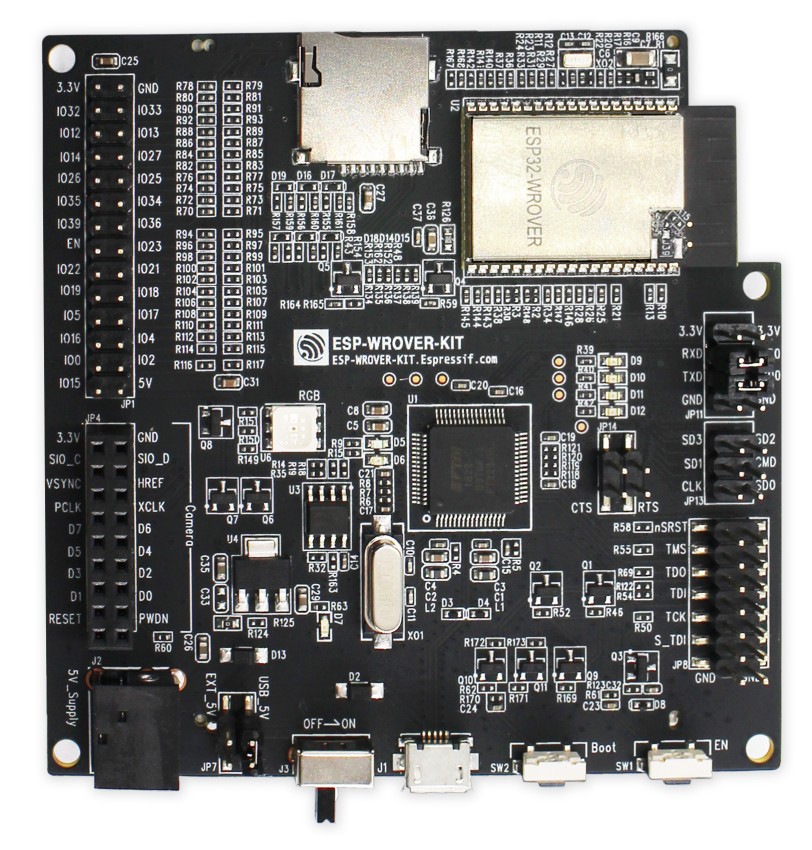
Board Pinout
The following picture shows the pinout of the ESP-WROVER-KIT V3 boards as defined by the default board configuration. The light green GPIOs are not used by configured on-board hardware components and can be used for any purpose. However, if optional off-board hardware modules are used, these GPIOs may also be occupied, see section esp32_wrover_kit_board_configuration for more information.
The corresponding board schematic can be found here.

Flashing the Device
Flashing RIOT is quite straight forward. The board has a Micro-USB connector with reset/boot/flash logic. Just connect the board using the programming port to your host computer and type:
BOARD=esp32-wrover-kit make flash ...The USB bridge is based on FDI FT2232HL and offers two USB interfaces:
- the first interface is the JTAG interface for On-Chip debugging
- the second interface is the console interface, which is also used for flashing
Therefore, you have to declare the USB interface in the make command. For
example, if the ESP32-WROVER-KIT is connected to the host computer through the
USB interfaces /dev/ttyUSB0 and /dev/ttyUSB1, the make command would be
used as following:
BOARD=esp32-wrover-kit PORT=/dev/ttyUSB1 make flash ...For detailed information about ESP32 as well as configuring and compiling RIOT for ESP32 boards, see esp32_riot.
On-Chip Debugging with the Device
Since the USB bridge based on FDI FT2232HL provides a JTAG interface for debugging through an USB interface, using ESP-WROVER-Kit V3 is the easiest and most convenient way for On-Chip debugging. Please refer the ESP-IDF Programming Guide for details on how to setup and how to use ESP-WROVER-Kit V3 and OpenOCD.
To use the JTAG interface, the esp_jtag module has to be enabled for
compilation.
USEMODULE=esp_jtag make flash BOARD=esp32-wrover-kit ...To flash and debug using OpenOCD, the precompiled version of OpenOCD for ESP32 has to be installed using the install script while being in RIOT’s root directory, see also section Using Local Toolchain Installation.
dist/tools/esptool/install.sh openocdBefore OpenOCD can then be used, the PATH variable has to be set correctly
and the OPENOCD variable has to be exported using the following command.
. dist/tools/esptool/export.sh openocdOnce the PATH variable and the OPENOCD variable are set, OpenOCD can be used
-
to flash the application using command
Terminal window PROGRAMMER=openocd USEMODULE=esp_jtag make flash BOARD=esp32-wrover-kit ... -
to start a debugging session (the board will be reset, but not flashed) using command
Terminal window PROGRAMMER=openocd USEMODULE=esp_jtag make debug BOARD=esp32-wrover-kit ...
by setting the PROGRAMMER variable to openocd.
Note: Even if the JTAG interface is used for debugging, the ESP32 standard
method for flashing with esptool.py can still be used. In that case, the
flash target is made without setting the PROGRAMMER variable.
Other Documentation Resources
There is a comprehensive Getting Started Guide for the ESP-WROVER-KIT with a lot information about hardware configuration.